

OLED Technology
OLEDs have been in the display market place for some time as PMOLEDs and have recently exploded into the market place with AMOLEDs. OLED stands for Organic Light Emitting Diode and provides the method of image production. OLEDs are different from LCDs in the fact that each individual pixel produces its own light instead of the light manipulation process of LCDs. With this feature OLEDs are capable of being very thin compared to backlight dependent technologies and are very attractive to wearable and other industries requiring minimal space for components of a product. AMOLED vs PMOLED is the technology used to drive the display with Active Matrix and Passive Matrix the AM and PM in the names. Active Matrix uses TFT technology to drive the individual pixels while PMOLED uses the external circuitry to drive each individual row and column at a time limiting the refresh rate. In the passive style pixels are primarily off during operating and to compensate each pixel must be driven at a higher brightness. The Passive Matrix limits the size and resolution of PMOLED technology.
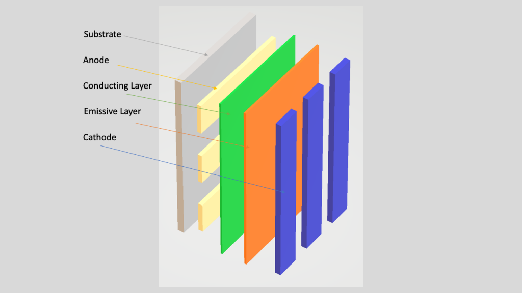
In the image above one can see the structure of an AMOLED and how the light is generated. From right to left:
- The Housing provides structural support to the module and varies depending on the module and application.
- The Substrate level provides support during the production process. The substrate in this example is clear glass and can vary in from module to module. Some use glass, clear glass, or plastic depending on the end goals of the module. In flexible OLEDs the substrate is a plastic film that is applied to a glass substrate. At the end of production, the plastic film (with OLED attached) will be removed from the glass during the delamination process using laser irradiation.
- The Anode layer (TFT) removes electrons (add electron “holes”) when current is applied to the OLED pixel.
- The Conducting layer is made of organic plastic molecules that transport the “holes” from the anode and commonly made out of polyaniline.
- The Emissive layer is the light emitting layer and commonly made out of polyfluorene. This layer transmits the electrons from the cathode.
- The Cathode can be transparent or not depending on the type of OLED being produced and this layer injects the electrons when current is applied to the pixels
Below is a breakdown of an individual OLED pixel including the individual organic layers:
There are three primary ways to apply the organic layers to the substrate:
- Vacuum deposition or VTE( Vacuum Thermal Evaporation) – This process is expensive and inefficient with organic molecules heated to evaporation and allowed to condense as thin films on cooled substrates inside a vacuum chamber.
- Organic Vapor Phase Deposition(OVPD) – A carrier gas is used to transport the organic molecules increasing the efficiency and lowering costs. This process is completed in a low pressure hot wall reactor chamber where the evaporated organic material is allowed to condense into thin films on the cooled substrates.
- Inkjet printing – Just like a printer the organic material is printed onto the substrate. This technology allows the manufacturing of large panels like tvs and billboards. This process greatly decreases the cost of manufacturing.
There are many benefits to using OLED technology in a project and OLEDs can make a product stand out compared to the competition. To get more information or discuss more information please Contact our team and we will be happy to help.
Leave a Reply